Documentation in the Assembly of Circuit Boards
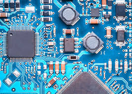
Printed circuit boards (PCB) are crucial to the function and performance of electronic devices. The assembly process for these intricate boards requires careful attention to detail and stringent quality control measures. In order to ensure the highest level of precision and accuracy, manufacturers must strictly adhere to industry standards throughout the manufacturing and assembly processes. Failure to do so could lead to defective or faulty products, which can potentially be hazardous for consumers and pose safety risks.
To produce a high-quality assembled circuit board, manufacturers must thoroughly examine each board for any potential flaws or irregularities before final assembly begins. This involves conducting thorough testing procedures alongside meticulous visual inspections. In addition, manufacturers must uphold stringent quality standards by sourcing components from reputable suppliers who prioritize compliance with industry norms and implementing environmentally conscious production practices.
When a PCB has been inspected and deemed acceptable for assembly, the next step is to apply a layer of copper onto its surface. This layer serves several important functions, including preventing solder bridges and protecting the surface of the board from environmental damage. Additionally, it allows for more accurate component placement by ensuring that the copper traces match the dimensions of the component footprints.
The Role of Documentation in the Assembly of Circuit Boards
Once the copper has been applied, a layer of epoxy resin is poured over it. The epoxy acts as a protective barrier for the copper and prevents moisture from damaging or weakening the boards. Finally, a layer of solder mask is applied to the board, which contains a thin, stainless-steel stencil that allows assemblers to accurately apply a precise amount of solder paste to designated areas of the would-be PCB where components will sit.
After the solder paste has been applied, the remaining components are inserted into the holes on the PCB. Thru-hole components are inserted by hand, and surface mount components are placed using a pick and place machine or selective soldering tool.
When designing a PCB, engineers must take into account the function and location of each component, as well as its physical characteristics. For example, the size and position of each hole must be carefully analyzed so that they don’t conflict with any other electrical traces or components on the board. The PCB layout must also be checked for errors, known as Design Rule Checks (DRC), to identify any potential problems.
To efficiently prepare a PCB for manufacture, manufacturers must have detailed documentation that includes the Bill of Materials (BOM), a Centroid File or Pick and Place file, and matching Gerber data. The BOM should include a list of all components, their reference designators, manufacturer part numbers, raw materials, packages and other information necessary for precise assembly on the board.
In addition to the BOM, manufacturers should also provide a file that lists all parts that shouldn’t be populated on the board, called a DO NOT POPULATE (DNP) file. Providing this information helps to speed up the assembly process and reduce costs by minimizing unnecessary work. It also helps to eliminate rework and production delays caused by inaccurate or incomplete data.